I destroyed and opened several Electret Condenser Microphones taken out from phone handsets.
Size roughly
Dia 10mm x H 5mm - 3pcs
Dia 8mm x H 4.5mm - 1pc
Dia 6 mm x H 2mm - 1pc
Dia 5mm x H 2mm - 2pcs (1pc not opened yet)
Dia 4mm x H 1.5mm - 1pc (not opened yet)from Blackberry)
I found
K596 and K596S in Dia 10 x H 5mm and Dia 8 x H 4.5mm Mics
Small three terminal part and two MLCCs in Dia 6mm x H 2mm Mics
Small three terminal part and one MLCC in Dia5mm x H 2mm Mic
The small three terminal part (cannot identify) highly likely has a similar function to that of K596(S) which is JFET.

When considering the number of Mobile Phones produced and sold and used - more than 1,000 million sets per year worldwide these small size Mics are produced and sold and used - more than 1,000 million pieces per year, too. But not just for Mobile Phones though dominant now. Plus non Cordless and convention Phones and some other applications using small size Microphones of this type the number may reach 1,500 million or more. Also so may do JFETs ? And why JFET ?
Electret Condenser Microphone is a remarkable invention. To get an idea.
Wiki : Elecret Microphone
"
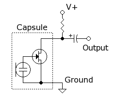
A typical electret microphone preamp circuit uses an FET in a common source configuration. The two-terminal electret capsule contains a FET which must be externally powered by supply voltage V+. The resistor sets the gain and output impedance. The audio signal appears at the output, after a DC-blocking capacitor.
"
<
The resistor sets the gain and output impedance.> may be difficult to understand without some electrical knowledge.
This type of Mic is Mechatronics product or Transducer as the condenser part (the left hand circle) is a capacitor (two plates as shown in the symbol) and the capacitance value changes mechanically according to the change of voice (sound) air pressure, a kind of vibration like a dram surface. Then this capacitance change (containing voice/sound information) is transferred (transduced) through the current change to Voltage change at output (Vout), which transmit to another place (via wire or wireless) and further changes through some amplifier to make a speaker sound.
Capacitor part
V = Q/C
where Q is Charge of Capacitor and C is Capacitance (in Farad).
Q is fixed in case of Electret Condenser Mic so only the change of Capacitance produces the change of Capacitor Voltage accordingly.
C (Capacitance) = e (dielectric constant) x Area (of the plate) / distance (between the two plates)
<e (dielectric constant) x Area (of the plate)> is nearly constant so V changes according to the distance (between the two plates). This distance changes in accordance with the air pressure of voice or sound.
Now let us see JFET.
I checked the specs of several different suppliers like ON Semi (Formally Sanyo product), KEC (Korea), UTC (Taiwan), Jiangsu Changjian (China) - all having <596> and saying <for Electret Condenser Mic) and the specs (Data Sheets) are more or less the same. One spec of 2SK596 (FOSHAN BLUE ROCKET ELECTRONIC, China) shows Z (= impedance).
Zin f=1MHz 25 MΩ
Zo f=1MHz 700 Ω
This spec (available on te net) is very simple (one page spec with no experiment charts) so I cannot check at Zin at lower sound frequency but capacitor impedance usually higher at lower frequencies (less than 1MHz) , zero Frequency - DC impedance infinite or realistically may be some little DC current leak. But Audio frequency is usually
20 to 20,000 Hz (= 0.02MHz).
Wiki <JFET> says
"
A JFET has a large input impedance (sometimes on the order of 10
10 ohms)
"
10
10 ohms = 10,000,000,000 ohms = 10,000MΩ
Another feature is
Basic features of JFET is (also Wiki)
"
Unlike bipolar transistors, JFETs are exclusively voltage-controlled in that they do not need a
biasing current.
Electric charge flows through a semiconducting channel between
source and
drain terminals. By applying a reverse bias
voltage to a
gate terminal, the channel is "pinched", so that the
electric current is impeded or switched off completely.
"
(<By applying a reverse bias
voltage to a
gate terminal> . This part you recall a PN Junction Diode behavior)
and
"
A JFET is usually
ON
when there is no voltage between its gate and source terminals. If a
potential difference of the proper polarity is applied between its gate
and source terminals, the JFET will be more resistive to current flow,
which means less current would flow in the channel between the source
and drain terminals.
"
<no voltage between its gate and source terminals > can be shown as V
GS = 0.
Putting these in your head you can read the spec more meaningful but not enough. See the spec of K596 or 2SK996 or whatever <596>.
ON Semi 2SK596S
20V, 150 to 350uA. 1.0Ms, N-Channel
<N-Channel>means Negative Electrons go through Chanel from Source to Drain when apply Voltage called VDS (D+, S-) then "Current" flows from Drain to Source (the current arrow shows this direction)
"
By applying a reverse bias
voltage to a
gate terminal, the channel is "pinched"
"
In cease of <N-Channel>the reverse bias voltage is <negative> at Gate to the ground or to Source (VGS) and therefore negative to Drain.
The first line of the spec of Absolute Maximum Ratings at 25 Deg C
1. Gate to Drain Voltage max -20V (this may be Minimum as this is negative value or can be considered as Minus Maximum 20V>)
<Gate to Drain Voltage> is relative voltage since Drain Voltage is normally positive to the ground, and to Source as well (when the current is flowing). But V
GD appears only here and no related charts.
When this is more negative than -20 V what will happen ? Some article on FET shows the following <breakdown> charts.
http://www.learningaboutelectronics.com/Articles/What-is-the-breakdown-voltage-of-a-FET-transistor
What is the Breakdown Voltage, BVDS, of a FET Transistor?
(One article from <Types/Characteristics of JFETs>.)

This chart (not so accurate but good presentation as a tutorial. This article a not a profissional engineering writing) shows at any V
GS Breakdown occurs as VDS increases. 20V seems related but how to relate with the spec of
Absolute Maximum Ratings at 25 Deg C <Gate to Drain Voltage max -20V> ?
But this article
does explain why and how <breakdown> happens but the story is not so convincing. Why and how <saturation> and <breakdown> happen so regularly as shown in this chart ?
Another explanation
"
The JFET Breakdown region
A high
voltage
at the terminals of JFET transistor can lead to a breakdown through the
gate junction. The manufacturer specifications show the breakdown
voltage between the drain and the source terminals when the gate and the
source terminals are joined. This voltage is known as BVDSS and its
value is between 20 and 50 volts. These bias voltages do not have to be
greater than these values in order to avoid the deterioration of the
device.
"
This refers to <The manufacturer specifications>but <the breakdown
voltage between the drain and the source terminals when the gate and the
source terminals are joined. >
<the breakdown
voltage between the drain and the source>not <Gate to Drain Voltage >. But <(when) the gate and the
source terminals are joined>which means short, then what happens ?
The chart shows the current is up vertically while the voltage (VDS) remains like Zener Diode. Can be used this phenomenon for some application ?
2. Gate Current (I
G) : 10mA max
3. Drain Current (I
D) : 1mA max
4. Allowable Power Dissipation: 100mW max
The current and power are relatively small. If these were large JFET will be damaged (but how?)
----ー
Electrical Characteristics at 25 Deg C
1. Gate to Drain Breakdown Voltage I
G 100uA min -20V
0.1mA (100uA) x 20V = 2mW, which is small. So this breakdown is due to the voltage stress.
2. Cutoff Voltage V
GS(off) VDS 5V, ID= 1uA Typ -0.5V , max -1.0V
This means at VGS = - 0.5 to -1.0V ID becomes 0 (the current stops). When ID becomes 0 the output voltage becomes high. Please note <A JFET is usually ON
when there is no voltage between its gate and source terminals (VGS = 0).> and when VGS becomes typically -0.5V ID becomes 1uA or less.
<Condition: VDS 5V, ID= 1uA> may need some explanation. The experiment chart shows this but cannot see 1uA at VDS 5V. This can be used as a switch function, (voltage control) switch.
A JFET is usually ON - the output voltage is low (as the current flows at the output point)
When a JFET is Cutoff - the output voltage is high (as only a very small ID current or no current flows at the output point).
3. Drain Current IDSS VDS 5V, VGS 0V Rank A 150 - 240uA
Rank B 210 - 350uA
This should be <Saturated Drain Current> IDSS means ID saturated. (Why <ss>?).
IDSS (region) is important for (as) a honest transducer as even VDS increases IDSS remains the same level after passing Vp (Pinch-off VDS) while ID changes according to the change of VGSas shown in the above chart.
Why and how this (saturation) occurs ?
I found the following explanation (convincing) in the text book I have.
"
IDSS
Conversely
if (the) current ceased to flow at the pinch-off, the depletion region
would shrank and the current flow would resume. Of course the change is
current never actually occurs. ID simply remains at IDSS.
"
A kind of negative feedback reaction or equilibrium mechanism.
Constant current (I
D) against the voltage change (in this case V
DS) is required for some applications like LED, which is a current operated device. A smaller current - dimmer, larger current brighter, though limited. not only for keeping the constant brightness again change of V
DS, a voltage control dimmer is possible by using JFET.
4. Forward Transfer Admittance |Yfs| VDS 5V, VGS 0V, f = 1MHz min 0.4, typ 1.0 mS
This is a bit technical but this is analogous to hHE of Bipolar Tr but not the ration of Corrector I / Base I (no unit). See below.
"
https://www.tek.com/support/faqs/how-do-i-test-jfet-small-signal-forward-transfer-admittance-my-curve-tracer
Small Signal Forward Transfer Admittance - |Yfs|
What It Is:
Small
signal forward transfer admittance is the ratio of a change in ID to a
change in VGS, with the initial VGS value usually = 0. The (Delta I/
Delta V) ratio is commonly referred to as small signal
gain and is given
in units of mhos (Siemens).
"
Please note the condition of 1MHz.
Anyway <gain is nearly less than 1/1000 Siemens (1mA/1V = 1mS) , no gain. But this is dI/dV so the unit is mS (mili Siemens). You can see this ID-VGS (with different IDDS, and different temperatutres) Charts in the spec.
But the above charts do not say <the condition of 1MHz.>. However the spec shows
Chart of |Yfs| vs IDDS chart with the condition of VDS=5V, VGS=0V and f = 1MHz.
and
Chart of VGS (off) vs IDDS with the condition of VDS=5V, ID = 1uA
5. Input Capacitance Ciss VDS 5V, VGS 0V f = 1MHz Typ 4.1pF
This is an intrinsic capacitance <measured between the gate and source terminals with the drain shorted to the source of AC signals, made up of the gate to drain Capacitance CGD in parallel with the gate to source Capacitance CGS, or CISS = CGD + CGS >
6. Reverse Transfer Capacitance
Crss VDS 5V, VGS 0V, f = 1MHz Typ 0.88pF
This
is also an intrinsic capacitance <measured between the drain and gate terminals with the source shorted to the ground. This is equal to the gain to drain capacitance.>
5. Input Capacitance and 6. Reverse Transfer Capacitance are much smaller than those of MOSFET due to to the structure difference. This is one of the reasons why JFET is used for Electret Condenser Mic.
"Radioworld" <Design and Performance of Electret Condenser Microphones> (a good article on this issue)
https://www.radioworld.com/news-and-business/design-and-performance-of-electret-condenser-microphones
of-electret-condenser-microphones) says:
"
Fig. 8: Low-cost electret condenser microphones almost
universally contain a JFET in the capsule. The capacitive electret
element has virtually no resistance and a capacitance of only 30 to 80
picofarads. Only a junction field-effect transistor gate has an input
resistance high enough to avoid loading down the signal from the
condenser element. The JFET source is typically grounded and the drain
is pulled up by a resistor (external or internal), resulting in a
“phantom bias” on the gate junction. Gain of the JFET is slightly less
than unity. EXAMINING LOW-COST ELECTRET TRANSDUCERS
One of the attractions of electret microphones is their low cost.
Another is their potentially small size, as shown in Fig. 6 (one in cell
phones may be as small as 2 mm in diameter!). However, the low cost and miniaturization of electret condenser
microphones had to wait until the Field Effect Transistor became
available (with its extremely high input gate impedance, compared to
bipolar transistors) to replace electron-tube impedance converters. The
FET allowed Sony (and others) to produce an electret microphone at a
price low enough to use with battery-operated recorders.
"
The first bold type part.
"
Only a junction field-effect transistor gate has an input
resistance high enough to avoid loading down the signal from the
condenser element.
"
This explains why JFET, not MOSFET, is used for this application. But MOSFET has this property too.
“phantom bias” - What is this ?
Found on the net (Why JFET and not MOSGET for Electret Condenser Mic).
Please see below:
https://electronics.stackexchange.com/questions/432504/why-are-the-advantages-of-jfet-over-mosfet-or-why-are-jfet-still-used
The JFET has several advantages over the MOSFET. The most important are:
- 1) higher gain
- 2) lower noise
3) These are the overriding factors when building preamplifiers for low-level signals, such as those from microphones.
4) Also, since there's no thin gate oxide that can be punctured by ESD, they're a little more "rugged" in that sense.
5) JFETS have a useful biasing, like a vacuum tube biasing.
Simply place a 100 ohm resistor in the Source pin to Ground to control
the current, and you can then connect Gate to a DC_conducting sensor
such as Moving Coil vinyl-record cartridges
and enjoy the JFET response down to DC with no need for DC_blocking
capacitors.
DC Bias
https://forum.allaboutcircuits.com/threads/why-electret-microphones-use-jfet.151848/
6 ) The capacitance of the electret part is quite small, and the charge
delivered is really tiny. So the device to connect to it must therefore
have a very small amount of charge required to produce a useful output. A
Jfet is the easiest solution. All of the other options are far more
expensive and far less convenient.
----ー
The spec continues.
Voltage gain:
Reduced voltage Characteristic
Frequency Characteristic
Total Harmonic Distortion (THD)
Output Noise Voltage
These are important as these are closely related with the spec of Electret Condenser Mic.
sptt